
[Update May 2023: this work was featured in IEEE Micro magazine, volume 43, issue 3. If you’re a subscriber, you can read the issue here To download a pdf of the article, click here.]
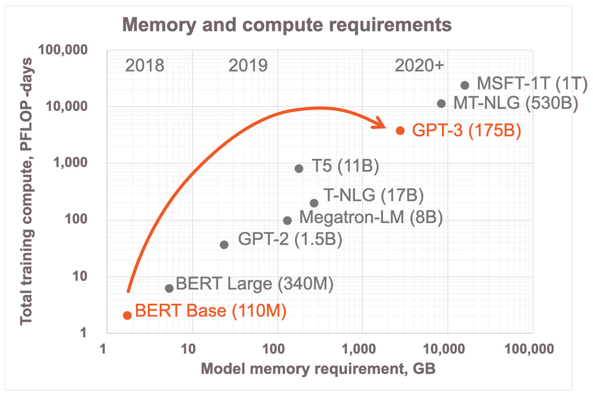
Neural networks have grown exponentially in recent years, from 2018 state-of-the-art neural networks of 100 million parameters to the famous GPT-3 with 175 billion parameters. However, this Grand ML Demand Challenge must be addressed by making substantial improvements — an order of magnitude or more — across a broad spectrum of multiple different components. This post is a written version of a talk I gave at the Hot Chips 34 conference recently. It gives a deep dive into the Cerebras hardware to show you how our revolutionary approaches in core architecture, scale-up, and scale-out are designed to meet this ML demand.
The Grand ML Demand Challenge
We’re just at the beginning of tapping into what neural networks can do. We’re also already reaching a pace where traditional approaches to training and inference just can’t keep up. In 2018, state-of-the-art neural networks had 100 million parameters, and that was a lot. Fast forward two years later, and we get the famous GPT-3 with 175 billion parameters. There’s no end in sight; tomorrow we will want to run models with trillions of parameters. That’s over a thousand times more compute in just two years; over three orders of magnitude more compute in just two years (Figure 1).
This is the Grand ML Demand Challenge in front of us all. At Cerebras, we believe that we can meet this unprecedented demand. We can’t do it by relying on just a single solution. It must be addressed by making substantial improvements — order of magnitude or more — across a broad spectrum of multiple different components. To meet this unprecedented demand, we need order of magnitude improvements in the core architecture performance so we can go beyond just brute force flops. We need order of magnitude improvements scaling up; Moore’s Law simply isn’t enough. We need order of magnitude improvements in scaling out, to improve and simplify clustering substantially. All of that is required for us to have any hope of keeping up with this ML demand.
Is this even possible? It is, but only with an architecture that’s co-designed from the ground up specifically for neural networks. In this post, I’m going to take a deep dive into the Cerebras architecture to show you how we do this.
Core Architecture
First, at the heart of all computer architecture is the compute core. At Cerebras, we set out to architect a core that’s specially designed for the fine-grained, dynamic sparsity in neural networks.
This is a small core design, quite literally (Figure 2). It’s only 38,000 square microns in size and half of that silicon is used by 48 kilobytes of memory. The other half is logic, made up of 110,000 standard cells. The entire core runs at an efficient 1.1 gigahertz clock frequency and consumes only 30 milliwatts of peak power.
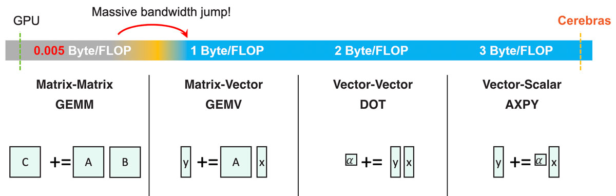
Let’s take a closer look at the memory. Traditional memory architectures such as GPUs use shared central DRAM, but DRAM is both slow and far away when you compare that to the compute performance. Even with advanced, bleeding-edge techniques like interposers and High Bandwidth Memory (HBM), the relative bandwidth from memory is significantly lower than the core datapath bandwidth. For example, it’s very common for compute datapaths to have 100 times more bandwidth than the memory bandwidth. This means each operand from a memory must be used at least 100 times in the datapath to keep utilization high. The traditional way to handle this is by using data reuse through local caching or local registers. However, there is a way to get full memory bandwidth to the datapaths at full performance, and that’s by fully distributing the memory right next to where it’s being used. This enables memory bandwidth that is equal to the operand bandwidth of the core datapath. The reason this is possible is, quite frankly, just physics. Driving bits tens of microns from local memory to the datapath, across silicon, is much easier than through a package to an external device.
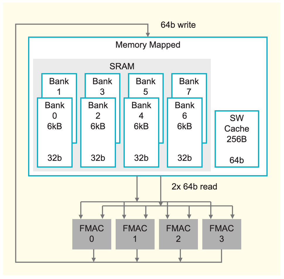
Next, let’s look at how this memory is designed (Figure 3). Each small core has 48 kilobytes of local SRAM dedicated to the core. That memory is designed to have the highest density while still providing full performance. This density and performance are achieved by organizing the memory into eight single-ported banks that are each 32-bit wide. With that degree of banking, we have more raw memory bandwidth than the datapath needs. So, we can maintain full datapath performance directly out of memory: that’s two full 64-bit reads, and one full 64-bit write per cycle. It’s important to note that all this memory is independently addressed per core. There’s no shared memory in the traditional sense. To enable truly scalable memory, all the sharing between cores is done explicitly through the fabric. In addition to the high-performance SRAM, we also have a small 256-byte software-managed cache that’s used for frequently accessed data structures such as accumulators. This cache is designed to be physically very compact and close to the datapath so that we can get ultra-low power for these frequent accesses. With this distributed memory architecture, we’re able to achieve a mind-boggling level of memory bandwidth. If you normalize to the GPU area, that’s 200 times more memory bandwidth within the same GPU area, directly to the datapaths.
Full Performance at All BLAS Levels
Now, with that level of memory bandwidth, we can do some remarkable things. We can run matrix operations out of memory, at full performance across all BLAS levels (Figure 4). Traditional CPU and GPU architectures with limited off-chip memory bandwidth are limited to running only GEMMs at full performance: that’s matrix-matrix multiplies only. In fact, you can see that any BLAS level below full matrix-matrix multiply requires a massive jump in memory bandwidth. That’s not possible with traditional architectures, but with enough memory bandwidth, you can enable full performance all the way down to AXPY, which is a vector-scalar multiply. Within neural network computation this is important because it enables fully unstructured sparsity acceleration. That’s because a sparse GEMM is just a collection of AXPY operations, with one operation for every non-zero element. This level of memory bandwidth is a prerequisite for unstructured sparsity acceleration. Additionally, we need a compute core that can accelerate that sparsity.
The foundation of the Cerebras core is a fully programable processor that can be made to adapt to the changing fields of deep learning. Like any general-purpose processor, it supports a full set of general- purpose instructions that includes arithmetic, logical, load/store, compare, and branch instructions. These instructions are fully local to each core, stored in the same 48 kilobytes of local memory as the data. This is important because it means every one of these small cores is independent. That enables very fine-grained, dynamic computation, globally across the entire chip. These general-purpose instructions operate on 16 general-purpose registers, and they run in a compact six-stage pipeline.
On top of this general-purpose foundation, we have hardware support for tensor instructions that are intended for all data processing. These tensor ops execute on the underlying 64-bit datapath, which is made up of four FP16 FMAC units. To optimize for performance and flexibility, our ISA has tensors as first-class operands, just like general-purpose registers or memory. Equation 1 shows an example of an FMAC instruction that’s operating on 3D and 2D tensor as operands directly.
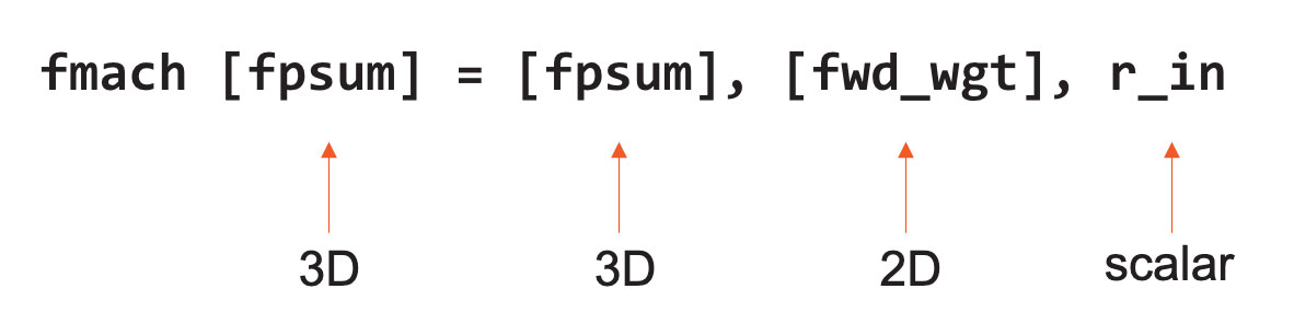
We do this by using data structure registers (DSRs) as operands to the instructions. Our core has 44 of these DSRs, each of which contains a descriptor with a pointer to the tensor and other key information such as length, shape, and size of that tensor. With this DSR, the hardware architecture is flexible enough to natively support up to 4D tensors that are in memory, or fabric streaming sensors, or FIFO, and circular buffers. Behind the scenes, there are hardware state machines that use the DSRS and sequence through the full tensor at full performance on the datapath.

Fine-Grained Dataflow Scheduling
On top of these tensor apps, the core uses fine-grained dataflow scheduling. Here, all the computation is triggered by the data (Figure 5). The fabric transports both the data and the associative control directly in the hardware. Once the cores receive that data, the hardware triggers a lookup of instructions to run. That look up is entirely based on what’s received in the fabric. With this dataflow mechanism in the cores, the entire compute fabric is a dataflow engine. This enables native sparsity acceleration because it only performs work on non-zero data. We filter out all the zero data at the sender, so the receiver doesn’t even see it. Only non-zero data is sent, and that’s what triggers all the computation. Not only do we save power by not performing the wasted compute, but we get acceleration by skipping it and moving on to the next useful compute. Since the operations are triggered by single data elements, this supports ultra-fine-grained, fully unstructured sparsity without any performance loss. To complement the dynamic nature of dataflow, the core also supports eight simultaneous tensor operations, which we call micro-threads. These are independent tensor contexts that the hardware can switch between on a cycle-by-cycle basis. The scheduler is continuously monitoring the input and the output availability for all the tensors that are being processed. It has priority mechanisms to ensure that the critical work is prioritized. Microthreading drives up utilization when there is a lot of a lot of dynamic behavior by switching to other tasks when there would otherwise be bubbles in the pipeline.
With this fine-grained, dynamic, small-core architecture, we can achieve unprecedented compute performance, as high as ten times greater utilization than GPUs on unstructured, sparse compute, or potentially even more with higher sparsity. Coming back to the grand challenge in front of us, this is how we can get an order of magnitude level improvement from the core architecture.
Scale-Up: Amplifying Moore’s Law
Now, let’s look at how we scale that up. Traditionally, scaling up within a chip has been the domain of the fabs. Moore’s Law has carried our industry for decades, enabling denser and denser chips. Today, Moore’s Law is still alive and well. But it’s only giving incremental gains, maybe a two times improvement per process generation, and that’s simply not enough. So, we ask ourselves, can we amplify Moore’s Law, and get an order of magnitude or more improvement?
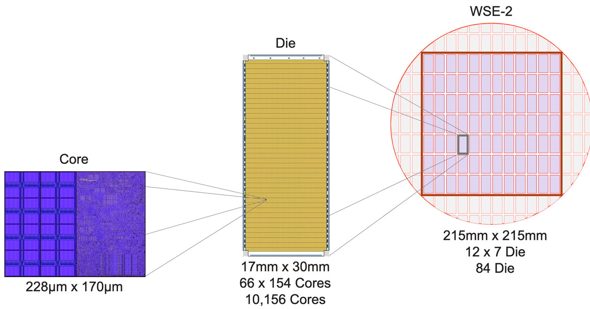
The traditional way to amplify Moore’s Law is to make larger chips. We did that, and we took it to the extreme. The result is our second-generation Wafer-Scale Engine, the WSE-2. It’s currently generally available and being used by our customers every day. It’s the largest chip ever built, at 56 times larger than the largest CPU today. It’s over 46,000 square millimeters in size, with 2.6 trillion transistors on a single chip, and we can fit 850,000 cores. With all those cores integrated on a single piece of silicon, we get some truly mind-boggling numbers for memory and performance because everything is on-chip.
We built a specially designed system around it, called the Cerebras CS-2. This was co-designed around the WSE-2, enabling the wafer-scale chip to be used in a standard datacenter environment. It’s truly cluster-level compute in a single box.
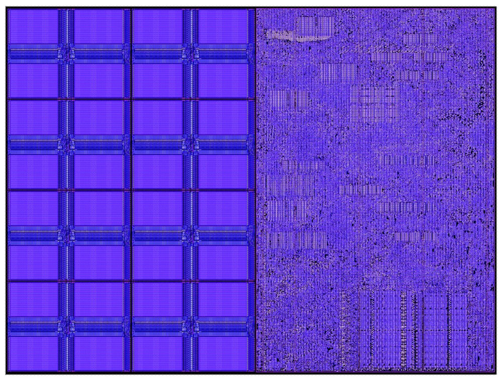
Here’s how we build up to that massive wafer from all those small cores. First, we create a traditional die with 10,000 cores each. Instead of cutting up those die to make traditional chips, we keep them intact, but we carve out a larger square within the round 300-millimeter wafer. That’s a total of 84 die, with 850,000 cores, all on a single chip (Figure 6.). All of this is only possible if the underlying architecture can scale to that extreme size.
The fundamental enabler is the fabric. It needs to enable efficient and high-performance communication across the entire wafer (Figure 7). Our fabric does this by using a 2D mesh topology that is well-suited to scale on silicon with extremely low overheads. This fabric ties together all the cores, where each core has a fabric router within the mesh topology. The fabric routers have a simple 5-port design with 32-bit bi-directional interfaces in each of the four cardinal directions and one port facing the core itself. This small port count enables single clock cycle latency between nodes, enabling a low-cost, lossless flow control with very low buffering.
The fundamental data packet is just a single FP16 data element optimized for neural networks. Along with that FP16 data, there are 16 bits of control information making up a 32-bit ultra-fine-grained packet. To optimize the fabric further, it uses entirely static routing, which is extremely efficient and low overhead, while perfectly exploiting the static connections of neural networks. To enable multiple routes on same physical link, we have 24 independent static routes that can be configured. We call those colors. All of them are non-blocking between one another and they’re all time-multiplexed onto
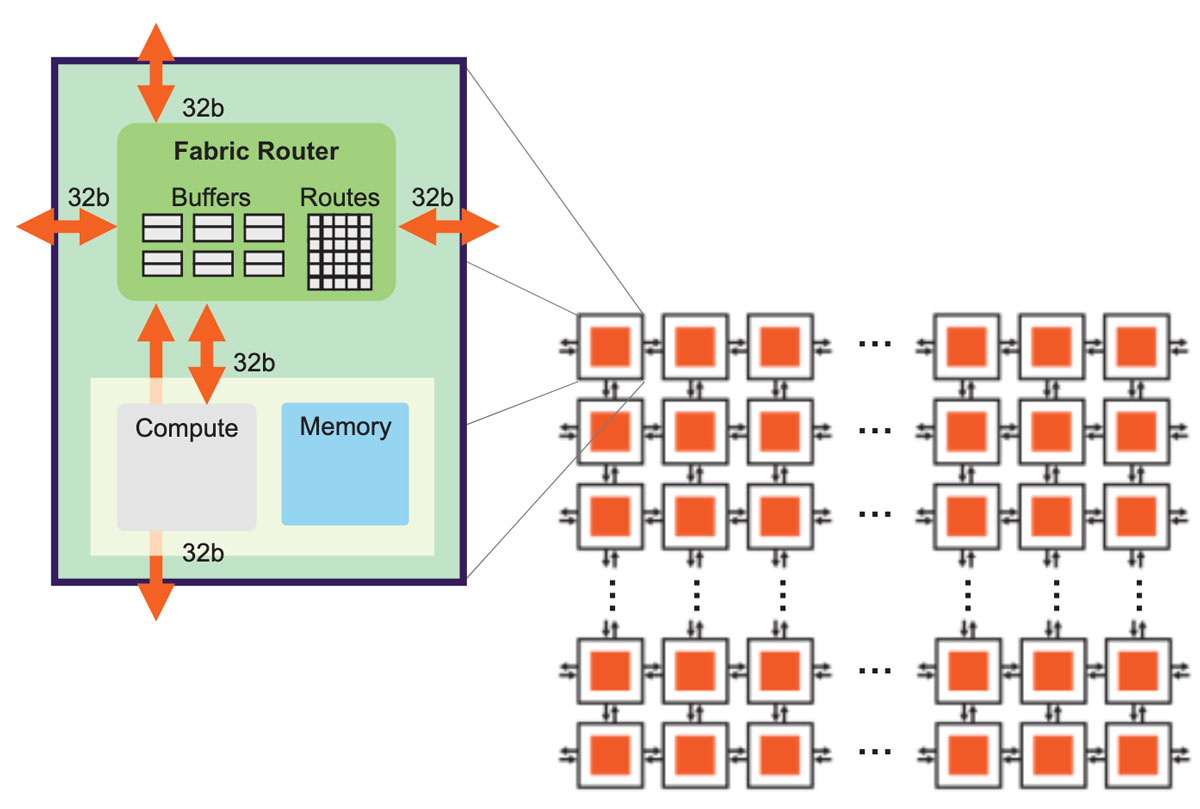
the same physical links. Lastly, neural network communication inherently has a high degree of fan-out, so our fabric is assigned with native broadcast and multi-cast capabilities within each fabric router.
Now that we have a scalable foundation, we need to scale it. Scaling within a single die is simple. To scale beyond the die, we extend the fabric across those die boundaries. We cross less than a millimeter of scribe line, and we do this using high-level metal layers within the TSMC process. This extends that to the 2D mesh compute fabric to a fully homogeneous array of cores across the entire wafer. The die-to- die interface is a highly efficient, source-synchronous, parallel interface. But, at this wafer scale, it adds up to over a million wires, so we must have redundancy built directly into the underlying protocol. We do that with training and auto-correction state machines. With these interfaces, even with defects in the fab process, we get a fully uniform fabric across the entire wafer.
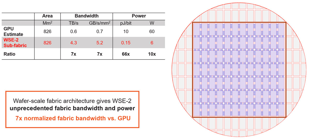
These seemingly simple short wires are a big deal because they span less than a millimeter of distance on silicon. When you compare that to traditional SERDES approaches, the difference is massive. Just like the memory, it’s just physics. Driving bits less than a millimeter on chip is much easier than across package connectors, PCBs, and sometimes even cables. This results in orders of magnitude improvement compared to traditional IO. As you can see from the table in Figure 8, we’re able to achieve about an order of magnitude more bandwidth per unit area, and almost two orders of magnitude better power efficiency per bit. All of this translates into unprecedented fabric performance across the entire wafer. If you normalize to GPU equivalent area, that’s seven times more bandwidth than GPU die-to-die bandwidth in the same GPU area, at only five watts of power. It’s this level of global fabric performance that enables the wafer to operate as a single chip. That’s important because with such a powerful single chip, we can solve some really, really large problems.
Weight Streaming Enables the Largest Models
The fabric enables us to run extremely large neural networks all on a single chip. The WSE-2 has more than enough performance and capacity to run even the largest models without partitioning or complex distribution. This is done by disaggregating the neural network model, memory weights, and the compute. We store all the model weights externally in a device called MemoryX, and we stream all those weights onto the CS-2 system as they’re needed to compute each layer of the network, one layer at a time. The weights are never stored on the system, not even temporarily. As the weights stream through, the CS-2 performs the computation using the underlying dataflow mechanisms in the cores (Figure 9).
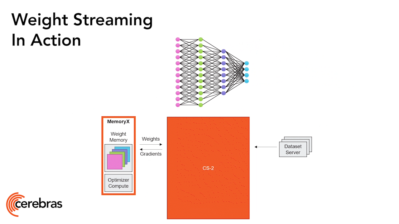
Each individual weight triggers the computation as an individual AXPY operation. Once each weight is complete, it’s discarded, and the hardware moves on to the next element. Now, since the weights are never stored on the chip, the size of the model is not constrained by the memory capacity on chip. On the backward pass, the gradients are streamed out in the reverse direction back to the MemoryX unit, where the weight updates happen.
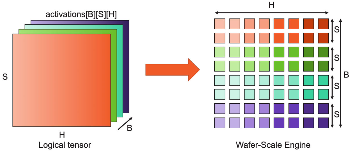
Let’s take a deeper dive into how the computation is performed, so we can see how the architecture properties uniquely enable this capability. Neural network layers boil down to matrix-multiplication. Because of the scale of the CS-2, we’re able to use all 850,000 cores of the wafer as a single, giant matrix multiplier (Error! Reference source not found.). Here’s how that works: For transformer models, like GPT, activation tensors have three logical dimensions: Batch, Sequence, and Hidden dimension (B, S and H). We split these tensor dimensions over the 2D grid of cores on the wafer. The Hidden dimension is split over the fabric in the x-direction and the Batch and Sequence dimensions are split over the fabric’s y-direction. This arrangement allows for efficient weight broadcast and reductions over Sequence and Hidden dimensions.
With activations stored on the cores where the work will be performed, the next step is to trigger the computation on those activations. This is done by using the on-chip broadcast fabric. That’s what we use to send the weights, the data, and the commands to each column. Of course, using the hardware dataflow mechanisms, the weights then trigger the FMAC operations directly. These are the AXPY operations. Since the broadcast occurs over columns, all cores containing the same subset of features receive the same weights. Additionally, we send commands to trigger other computations such as reductions or non-linear operations.
Let’s walk through an example. We start by broadcasting the row of weights across the wafer (Figure 11). Each element of the row is our scalar. Within that row, there are multiple weights that map onto a single column, of course. When there’s sparsity, only those non-zero weights are broadcasted to the column, triggering those FMAC computations. We skip all the zero weights, and we stream in the next non-zero weight. This is what produces a sparsity acceleration.

If we now zoom into a core, we can see how the core architecture is being used for this operation (Figure 12). When a weight arrives, using the dataflow mechanisms, it triggers an FMAC operation on the core. The weight value is multiplied with each of these activations and added into a local accumulator which resides in the SW-managed cache. The FMAC compute is performed using a tensor instruction with the activations as a tensor operand. All of this is done with zero additional overhead on the core. Additionally, there is no memory capacity overhead for the weights since once the compute done, the core moves onto the next weight. We never store any of the weights. Once all weights for the row have been received, each core contains a partial sum that needs to be reduced across the row of cores.
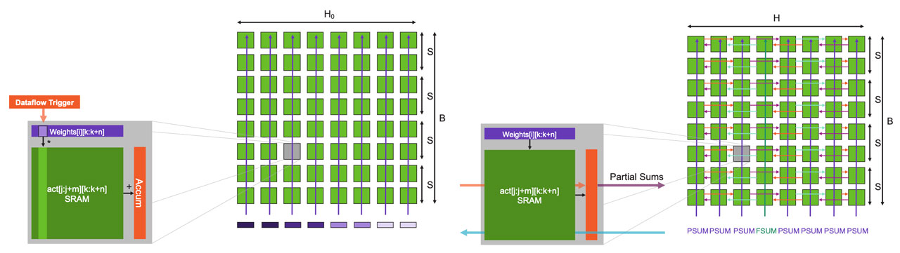
That reduction is then triggered by a command packet broadcasted to all the cores of each column. Again, using the dataflow scheduling mechanisms, once the core receives the command packet, it triggers the partial sum reduction. The actual reduction compute itself is done using the core’s tensor instruction, this time with fabric tensor operands. All the columns receive a PSUM (partial sum) command. But one column receives a special FSUM (final sum) command. The FSUM command indicates to the core that it should store the final sum. We do this so the output features are stored using the same kind of distribution as was used for input features, setting us up for the next layer. Once it receives the commands, the cores communicate using a ring pattern on the fabric which is set up using the fabric static routing colors. Using micro-threads, all this reduction is overlapped with the FMAC compute for the next weight row which started in parallel. Once all rows of weights are processed, the full GEMM operation is complete, and all our activations are in place for the next layer.
This enables neural networks of all sizes to run with high performance, all on a single chip. That’s made possible by the unique core memory and fabric architecture. This means extremely large matrices are supported without blocking or partitioning, even the largest models with up to 100,000 by 100,000 MatMul layers can run without splitting up the matrix. When you bring this together across the single WSE-2 chip, this results in 75 petaflops of FP16 sparse performance (and potentially even more with higher sparsity), or 7.5 petaflops of FP16 dense performance, all on a single chip. Now, bringing this back to the Grand ML Demand challenge in front of us, this is how we can achieve an order of magnitude level improvement in scaling up.
Scale-Out: Why Is it So Hard Today?
Let’s talk about the last component: Cluster scale-out. Clustering solutions already exist today. So why is it still so hard to scale?
Let’s look at existing scale out techniques (Figure 13). The most common is data parallel. This is the simplest approach, but it doesn’t work well for large models because the entire model needs to fit in each device to solve that. To solve that problem, the common approach is to run model parallel. This splits the model and runs different layers on different devices as a pipeline. But as the pipeline grows, the activation memory increases quadratically to keep the pipeline full. To avoid that, it’s also common to run another form of model parallel by splitting layers across devices. This has significant communication overhead, and splitting individual layers is extremely complicated. Because of all these constraints, there is no single one-size-fits-all way to scale out today. In fact, in most cases, training massive models requires a hybrid approach with both data parallel and model parallel. Although scale out solutions technically exist, they have many limitations. And the fundamental reason is simple: In traditional scale out, our memory and compute are tied to each other. Trying to run a single model on thousands of devices turns the scaling of both memory and compute into distributed constraint problems that are interdependent.

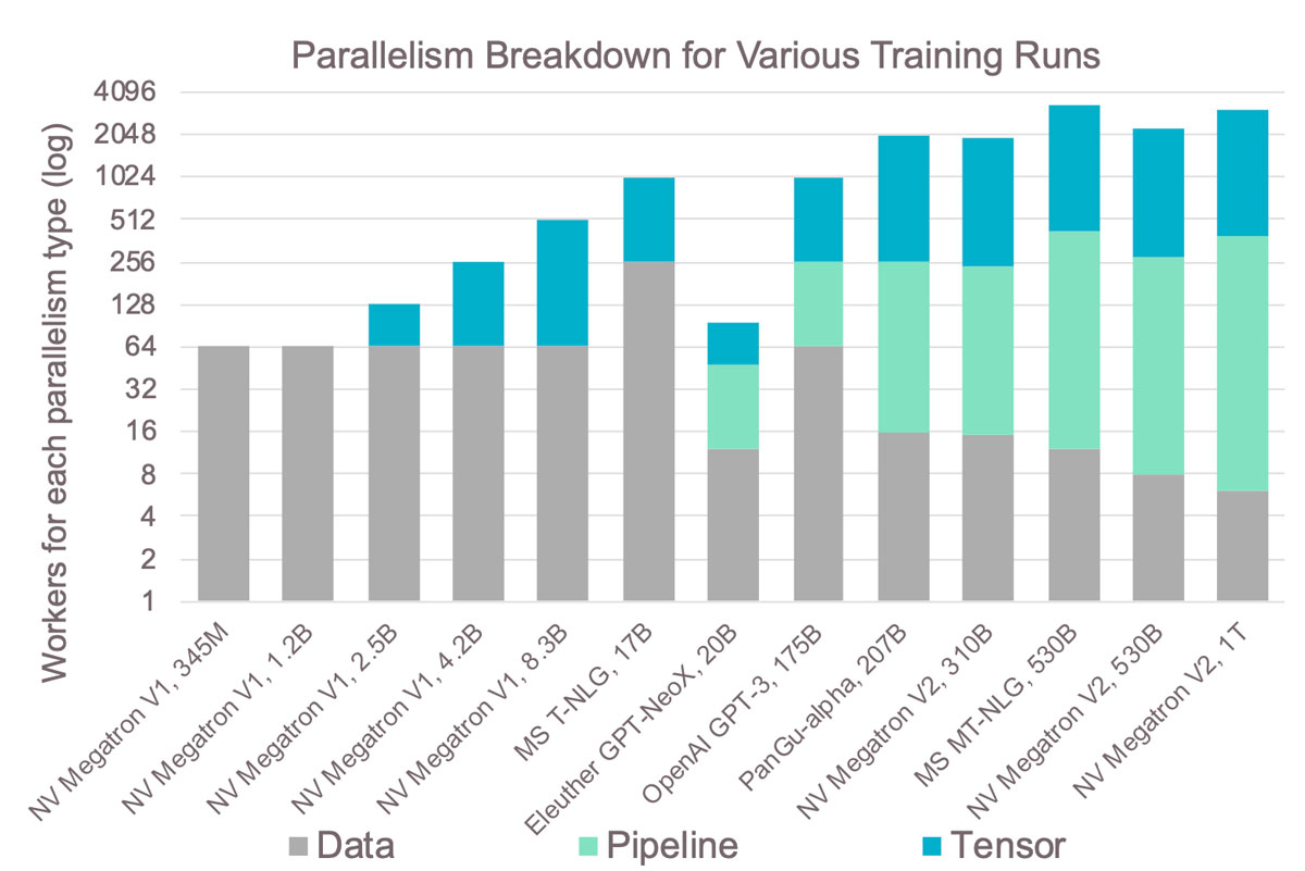
Here’s the result of that complexity: Figure 14 shows the largest models trained on GPUs over the last few years and the different types of parallelism used. As you can see, as the models get larger, the more types of parallelism are needed, and this results in a tremendous amount of complexity. For example, you can see that the level of tensor model parallelism is always limited to 8 because that’s the number of GPUs that are typically in a single server. As a result, most parallelism for large models is pipelined model parallelism, but that’s the most complex because of the memory tradeoffs. Training these models on GPU clusters today requires navigating all these bespoke distributed system problems. This complexity results in longer development times and often suboptimal scaling.
The Cerebras Architecture Makes Scaling Easy
On the other hand, because the Cerebras architecture enables running all models on a single chip without portioning, scaling becomes easy and natural. We can scale with only data parallel replication, no need for any complicated model parallel partitioning.
We do this with a specially designed interconnect for data parallel (Figure 15). This is called SwarmX. It sits between the MemoryX units that hold the weights and the CS-2 systems for compute but is independent from both. SwarmX broadcasts weights to all CS-2 systems and it reduces gradients from all CS-2s. It’s more than just an interconnect – it’s an active component in the training process, purpose- built for data parallel scale-out. Internally, SwarmX uses a tree topology to enable modular and low overhead scaling. Because it’s modular and disaggregated, you can scale to any number of CS-2 systems with the same execution model as a single system. Scaling to more compute is as simple as adding more nodes to the SwarmX topology and adding more CS-2 systems. That is how we address the last component of the Grand ML Demand Challenge; to improve and drastically simplify scale-out.

Conclusion
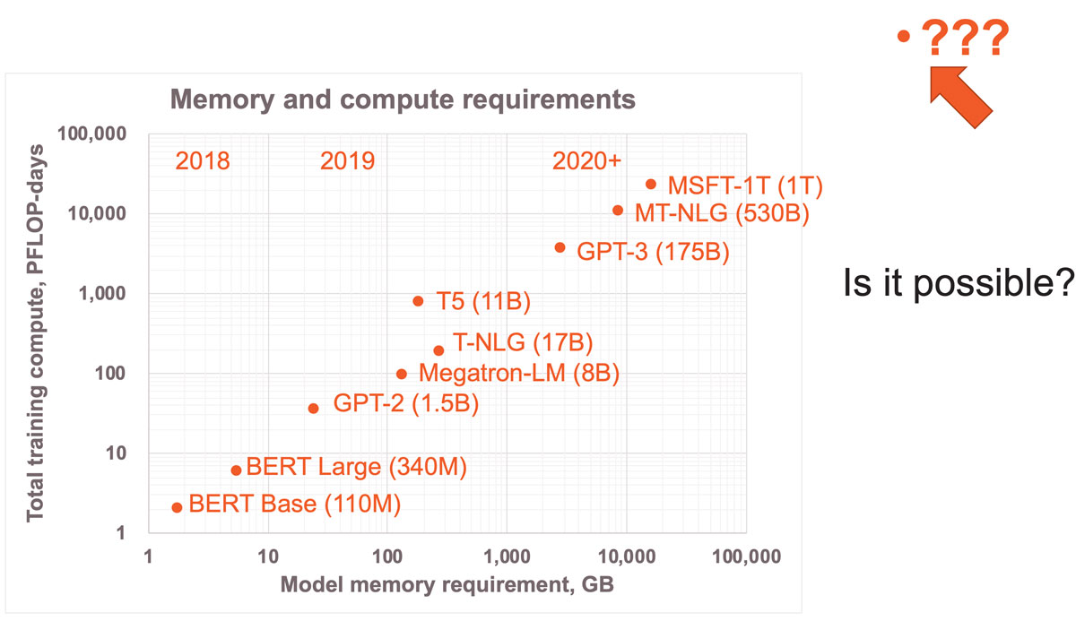
Let’s go back to where we started today. In the past couple of years, we have seen over three orders of magnitude greater demand from ML workloads, and there’s no sign of slowing down. In the next couple of years, this is where we will be (Figure 16). We ask ourselves, is this even possible?
At Cerebras, we know it is. But not by using traditional techniques. Only by improving the core architecture by an order of magnitude with unstructured sparsity acceleration. Only by scaling up by an order of magnitude with wafer scale chips, and only by improving cluster scale out by an order of magnitude with truly scalable clustering. With all of these, that future is achievable. Neural network models are continuing to grow exponentially. Few companies today have access to them, and that list is only getting smaller.
With the Cerebras architecture, by enabling the largest models to run on a single device, data parallel only scale out and native unstructured sparsity acceleration, we’re making these large models available to everyone.
Sean Lie, Co-Founder and Chief Hardware Architect | August 29, 2022
Recommended further reading:
Weight Streaming whitepaper A deeper dive into the technology of weight streaming, including a survey of existing approaches used to scale training to clusters of compute units and explore the limitations of each in the face of giant models.
Harnessing the Power of Sparsity for Large GPT AI Models A look at how Cerebras is enabling innovation of novel sparse ML techniques to accelerate training and inference on large-scale language models.
Related Posts

Cerebras CS-3 vs. Nvidia B200: 2024 AI Accelerators Compared
In the fast-paced world of AI hardware, the Cerebras CS-3 and Nvidia DGX B200…

Cerebras CS-3: the world’s fastest and most scalable AI accelerator
Today Cerebras is introducing the CS-3, our third-generation wafer-scale AI…